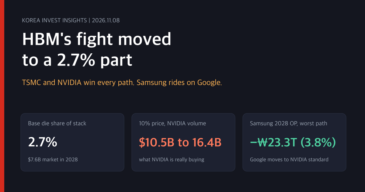
Open an HBM stack and the DRAM chips get the attention. Under them sits a logic chip called the base die, which handles the link to the GPU. Until now, memory makers designed it, and the contest between them was about DRAM cores: capacity, yield, speed. Now NVIDIA, the JEDEC standards body, TSMC, Marvell and Samsung are all putting more logic into it, and the contest is moving with it.
The catch is the size. In 2028 the base die is worth about $7.6 billion, 2.7% of an HBM market we assume at $282 billion. What it controls is larger. A 10% move in the price of NVIDIA’s HBM volume is $10.5 billion to $16.4 billion. The base die is a lever, and the prize is who sets the price.
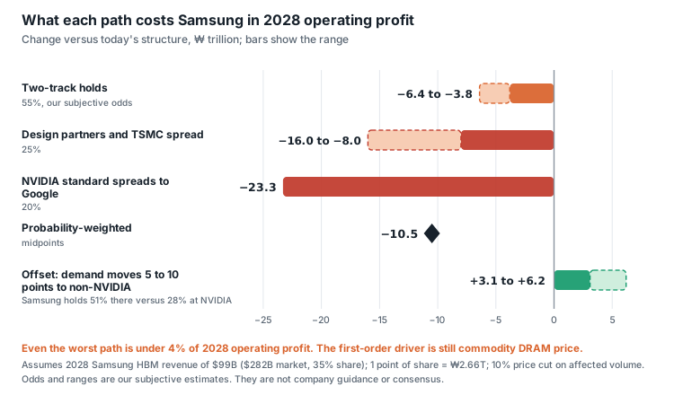
Our view: TSMC and NVIDIA win on every path we can draw. SK hynix loses part of its NVIDIA premium and AMD falls behind on every path. Broadcom, Google and Samsung rise or fall together on one variable: whether Google keeps its TPU memory outside NVIDIA’s NVLink Fusion. On our assumptions Samsung sells 51% to 76% of its HBM to non-NVIDIA buyers, the highest of the three makers, and Google alone is 23% to 47% of it. So Samsung’s loss is small if NVIDIA’s standard stays inside NVIDIA’s own volume, and large if Google crosses over. In our 2028 math that is a loss of ₩3.8 trillion to ₩6.4 trillion in the base case and ₩23.3 trillion (3.8% of operating profit) in the worst case. Even then, the first-order driver of Samsung’s profit is still commodity DRAM price.
- The base die is a $7.6 billion market. A 10% price move on NVIDIA’s HBM volume is bigger, which is why NVIDIA wants the design.
- Non-NVIDIA is no longer one camp. NVIDIA took a $2 billion stake in Marvell (March 31) and bought $3.5 billion of MediaTek convertible bonds (August 31). The real fault line is NVIDIA’s ecosystem against Broadcom’s camp.
- Our subjective odds for 2028: the two-track world holds at 55%, design partners and TSMC spread at 25%, NVIDIA’s standard spreads to Google or Meta at 20%.
- If memory makers must win back a 10% price cut with market share, SK hynix needs 5.8 points, Samsung 3.1 and Micron 2.2. The three needs add to 111%, so someone loses share.
- Samsung’s worst path costs 4 to 6 times its base case, and that asymmetry sits with Google.
A chip nobody watched is now where the fight is
An HBM stack is a tower of DRAM chips on a logic chip. For HBM4 and earlier generations, the memory makers designed the logic chip. Several designs now compete to take it over:
- NVIDIA’s NVHBM (announced August 26) moves the memory controller into the base die. It replaces the wide parallel bus of the JEDEC standard with a narrow serial link between dies, and it comes inside NVLink Fusion, NVIDIA’s program for connecting other companies’ chips to its network. Amazon’s Trainium4 is the first partner. NVIDIA’s performance claims are company statements.
- JEDEC’s own SPHBM4 (July 13) goes the same direction. It keeps the HBM4 DRAM dies, adds a new-interface base die with 4:1 serialization of 512 signals, and allows an organic substrate.
- TSMC and GUC offer a custom base die on N3P with about twice the efficiency (company materials via press). Marvell sells custom HBM4E with 2nm to 3nm logic in the base die. Samsung builds its own 4nm base die.
All of these narrow the parallel interface, so more logic moves into the base die. Whoever designs that logic controls the margin and the specification.
Who designs the base die decides who keeps the margin
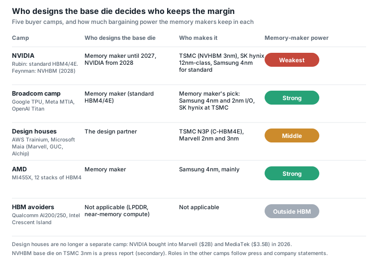
The question is who holds the pen. If the buyer designs the base die, as NVIDIA will from 2028, the memory makers become suppliers of a core die to a fixed design, and they are easy to swap. If a design partner designs it, the logic value moves to the partner and to TSMC. If the memory maker keeps it, as with standard HBM4 and 4E or Samsung’s turnkey offer, bargaining power stays with the memory maker.
TSMC is paid in all three cases. NVHBM’s base die, SK hynix’s 12nm-class base die, Micron’s HBM4E, C-HBM4E on N3P and CoWoS packaging all run through TSMC. The routes around TSMC are Samsung’s 4nm and 2nm base dies, Intel’s EMIB-T packaging, and SPHBM4 on organic substrates. All three sit on the non-NVIDIA side.
The money: a $7.6 billion part sets the price of the rest
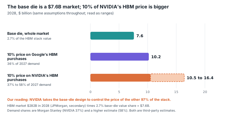
At a $282 billion HBM market (JPMorgan, secondary) and a 2.7% base-die value share, the base die is $7.6 billion. NVIDIA buys $105 billion to $164 billion of HBM in 2028 at a 37% to 58% demand share, so 10% of its volume price is $10.5 billion to $16.4 billion. Google’s 36% share makes 10% of its price worth $10.2 billion.
This is our reading of why NVIDIA wants the design. The reward is not base-die revenue. It is the ability to make three suppliers build the same part and compete on price. NVIDIA’s stake in that price is larger than TSMC’s whole base-die market.
NVIDIA’s play: own the standard
NVIDIA’s plan runs in three steps.
- 2026 to 2027, standard HBM4 and 4E. Memory makers design the base die. SK hynix’s work with TSMC gave it a performance edge, and SK hynix holds 54% of NVIDIA’s HBM in 2026 (JPMorgan, secondary).
- 2028, NVHBM. NVIDIA designs the controller and the die-to-die link, and a Seoul press report says the three makers build the same design on TSMC 3nm (secondary). SK hynix’s TSMC edge and Samsung’s 4nm edge both disappear on NVIDIA volume. What is left to compete on is core 1c yield, stacking and capacity. In our model, a 10% price cut on NVIDIA volume costs ₩4.9 trillion at Samsung, ₩6.3 trillion at SK hynix and ₩2.8 trillion at Micron in 2028 operating profit.
- 2029 and later, logic under the memory. A report on November 6 says TSMC is looking at 3D DRAM (business plan unconfirmed). SK hynix is also hiring in San Jose for 3D DRAM on logic and co-designing a logic die with a U.S. customer (secondary). If NVIDIA and TSMC design and make the logic layer under the cells, the memory maker’s share narrows to the cell array.
NVIDIA is also growing tiers outside HBM: SOCAMM (LPDDR) for inference, KV flash and Groq-style SRAM designs. A buyer that holds the design and the alternatives has the stronger hand.
Non-NVIDIA is not one camp
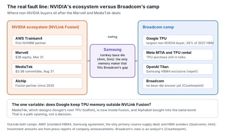
We first split non-NVIDIA demand four ways: Broadcom-centered hyperscalers, design-house custom chips, AMD, and HBM avoiders. Then two deals changed the map. NVIDIA took a $2 billion stake in Marvell on March 31, and on August 31 it bought $3.5 billion of MediaTek’s $3.9 billion convertible issue. MediaTek adopted NVLink Fusion for its own customers. Alchip, MediaTek and Marvell were also on Fusion’s first list of custom-compute partners in 2025. JPMorgan reads the Marvell deal as confirming Marvell as AWS’s Fusion integration partner (analyst reading).
So design houses are no longer an independent camp. The practical split is between NVIDIA’s ecosystem and Broadcom’s camp.
- Broadcom’s camp is the biggest non-NVIDIA demand. Alphabet alone is 36% of 2027 HBM demand (Morgan Stanley). Broadcom’s CoWoS allocation grows from 230,000 to 350,000 wafers in 2027 (JPMorgan, reported). This camp still uses standard HBM designed by the memory maker, which is where Samsung’s turnkey offer sells best. Reports have Samsung with more than 60% of Google’s HBM3E, an exclusive on OpenAI’s Titan HBM4, and a 2nm memory I/O die on MediaTek’s next Google TPU (all secondary, claims). Counterpoint calls Broadcom the last big design house NVIDIA has not joined, and says it has no base-die answer (analyst view). That is the gap Samsung’s 4nm and 2nm base dies can fill.
- AMD is the biggest single-chip buyer of standard HBM and Samsung’s first customer. The MI455X carries 432GB of HBM4 on 12 stacks. The March 18 AMD and Samsung agreement is the only primary-source supply deal in this story, and it includes talks on foundry cooperation. AMD is 12.1% of 2027 demand (Morgan Stanley).
- HBM avoiders cap the HBM premium. Qualcomm’s AI200 carries 768GB of LPDDR per card, and Intel’s Crescent Island carries 160GB of LPDDR5X. The bits stay in DRAM but outside HBM pricing. Orders are still small.
Google is the swing. It splits suppliers (Samsung, SK hynix), design (Broadcom, MediaTek) and packaging (TSMC, Intel EMIB-T from 2027, with a reported 2028 booking of more than 3 million TPUs). MediaTek, which designs Google’s next TPU, is now inside Fusion, and Alphabet joined the same bond offer. That opens a path to NVIDIA’s standard. It is not a decision, so we keep our odds where they were.
We also share new analyses on Telegram as they are published. You are welcome to join us at @korea_invest_insights.
Samsung is the most exposed to non-NVIDIA buyers
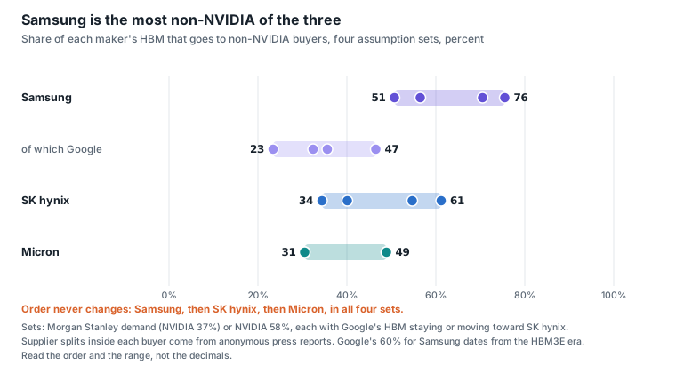
The formula is each buyer’s 2027 demand share times each maker’s split inside that buyer. The splits are assumptions fixed from press reports: NVIDIA (Samsung 28%, SK hynix 52%, Micron 20%), Google (55, 40, 5), AMD (60, 20, 20) and others (35, 45, 20). We ran two NVIDIA demand shares, 37% (Morgan Stanley) and 58%, and let Google’s volume either stay or move toward SK hynix.
The order never changes. Non-NVIDIA is the largest part of Samsung’s HBM, then SK hynix’s, then Micron’s. The shares these assumptions imply (Samsung 33% to 43%, SK hynix 43% to 50%, Micron 15% to 17%) come from the assumptions and do not test them.
NVHBM’s reach follows from the same table. NVIDIA alone is 37% of demand. Adding Amazon (about 5%, assumed) makes 42%, and adding Google makes 78%. If Google adopts NVIDIA’s standard, about 75% of Samsung’s HBM sits under it, against 25% with NVIDIA alone. Across the four cases the range is 70% to 81%. This assumes each buyer’s whole demand moves.
- SK hynix loses the most premium when NVIDIA neutralizes suppliers, because its NVIDIA share is high.
- Samsung’s risk sits with Google and Broadcom. The three triggers are whether Google adopts NVHBM, whether TPU HBM4 and 4E allocation tilts to SK hynix, and whether Broadcom’s custom base die goes to TSMC N3P.
- Micron has high NVIDIA exposure, but as the number three supplier it also gains from standard parts that lower qualification barriers.
What each path costs Samsung
| Path | What happens | Our odds | Why | Signal |
|---|---|---|---|---|
| Two-track holds | NVIDIA and Amazon use NVHBM. Google, Meta, OpenAI and AMD stay on standard or turnkey HBM | 55% | Google and Broadcom have their own interconnects and Broadcom’s Meta contract runs to 2029, so they have little reason to hand NVIDIA the spec. AMD has little reason to adopt a standard its rival controls | Google and Meta stay silent on NVHBM. Broadcom’s custom HBM keeps the memory maker’s design |
| Design partners and TSMC spread | Non-NVIDIA buyers also adopt C-HBM4E or Marvell-style custom parts, so memory makers supply core dies everywhere | 25% | N3P’s roughly 2x efficiency and Marvell’s view that HBM exceeds 50% of an XPU’s cost push buyers toward custom | Broadcom or Google picks a TSMC N3P custom base die. Meta’s MTIA gets custom HBM |
| NVIDIA standard spreads | Google or Meta adopts NVLink Fusion and NVHBM | 20% | Amazon already did, and NVIDIA wants Google too (secondary). Against that, Google is widening supply with EMIB-T, MediaTek and Samsung’s 2nm | Partner list at the December 2 event. Google’s next TPU memory spec |
Because Marvell and MediaTek are now inside Fusion, much of the second path can play out inside NVIDIA’s ecosystem. We keep the odds, but Samsung’s two bad paths, 45% together, are best read as one risk.
The cost on each path, using $99 billion of Samsung 2028 HBM revenue ($282 billion market, 35% share), ₩2.66 trillion of operating profit per point of share, a 10% price cut on affected volume, and a base die worth 2.7% of the stack at a 60% contribution margin:
- Two-track holds: 29% to 48% of Samsung’s HBM (NVIDIA and Amazon volume) loses 10% of price. That is −₩3.8 trillion to −₩6.4 trillion, 0.6% to 1.0% of 2028 operating profit.
- Design partners spread: the above, plus ₩1.55 trillion of base-die foundry contribution profit, plus 1 to 3 points of share lost with the turnkey advantage. That is −₩8.0 trillion to −₩16.0 trillion, 1.3% to 2.6%.
- NVIDIA standard spreads: 75% of volume loses 10% of price (₩10.0 trillion), Google’s share of Samsung falls from 55% to 40% (5.4 points of market, ₩14.4 trillion), Google’s base die is worth ₩1.0 trillion, and we subtract ₩2.1 trillion for double-counting the price loss on volume already lost. That is about −₩23.3 trillion, 3.8%.
- Probability-weighted, using range midpoints, about −₩10.5 trillion, 1.7%.
The base case is small because the loss lands where Samsung’s share is lowest (28% of NVIDIA’s volume) and the growth lands where its share is highest (51% of non-NVIDIA volume). If demand moves 5 points from NVIDIA to non-NVIDIA buyers, Samsung’s share rises 1.2 points and operating profit rises ₩3.1 trillion. A 10-point move gives 2.3 points and ₩6.2 trillion. Counterpoint expects HBM demand for ASIC compute to grow many times over by 2028 (secondary). If that shift happens, it offsets part or all of the base-case price loss. If it does not, the base case is negative.
The worst path is the tail. If Google moves to NVIDIA’s standard, or tilts HBM4E toward SK hynix, the damage is about 4 to 6 times the base case.
There is a foundry leg too. In the base case Samsung keeps the base-die foundry business for non-NVIDIA volume, about ₩2.6 trillion of internal revenue in 2028 (excluding Amazon) and about ₩1.55 trillion of contribution profit. That equals about 40% of our estimated 2026 foundry and LSI loss of ₩3.92 trillion. On the second and third paths that revenue shrinks, and one support for the foundry breakeven case weakens.
All three paths are 0% to 4% of 2028 operating profit. The first-order driver of Samsung’s profit is still commodity DRAM price, and HBM structure is second-order. It is, however, one of the biggest items separating Samsung from SK hynix in relative terms.
What changes for Samsung’s HBM story is its aim. With HBM4, Samsung used a 1c core and its own 4nm base die, more advanced logic than SK hynix’s TSMC 12nm-class die, and its HBM share rose from 21% in 1Q26 to 33% in 2Q26 (Counterpoint). Under NVHBM the base die is TSMC 3nm for everyone, and SK hynix moves to 1c from HBM4E. On NVIDIA volume Samsung’s weapons shrink to core yield, capacity and stacking. The story becomes standard and turnkey supply to non-NVIDIA buyers, and that business only exists outside NVIDIA.
Who wins on which path
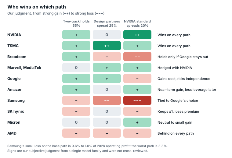
TSMC and NVIDIA do not lose on any path. AMD is behind on all three. Broadcom and Samsung move together: both are safe in the base case and lose in the other two.
| Company | What it gets | What it risks | What flips it |
|---|---|---|---|
| NVIDIA | Control of the base-die spec. Three makers on one design lower switching cost. Binds Amazon, Marvell, MediaTek and Alchip through Fusion | More dependence on TSMC 3nm. If non-NVIDIA buyers stay on memory-maker designs or SPHBM4, NVHBM stays inside its own camp. First-generation serial-link execution risk | Google and Meta absent from the December 2 partner list limits the win to its own volume |
| TSMC | NVHBM 3nm, SK hynix 12nm-class, Micron HBM4E, C-HBM4E N3P and CoWoS. The base die ties customers closer | Google’s EMIB-T and Intel packaging, SPHBM4 on organic substrates, Samsung’s 2nm I/O die. All of these are on the non-NVIDIA side | Intel confirms EMIB-T for Google. Broadcom’s custom base die goes to Samsung |
| Broadcom | The last big design house outside NVIDIA’s orbit (Counterpoint view). The main option for Google, Meta and OpenAI to stay outside NVIDIA | No base-die answer. If the base die becomes the differentiator it depends on Samsung’s turnkey offer or TSMC. MediaTek, Google’s second TPU designer, is inside Fusion | Google or Meta joins Fusion. Broadcom names a base-die partner on its fiscal fourth-quarter call |
| Marvell, MediaTek, Alchip, GUC | Marvell and MediaTek have NVIDIA money and Fusion access and still design custom chips for others. GUC has C-HBM4E | Marvell’s own custom HBM competes with NVHBM for the same customers. MediaTek must manage trust with Google and NVIDIA at once | How MediaTek’s Icefish connects, over Fusion or Google’s own network |
| The largest non-NVIDIA buyer with every supply layer split in two or more, which builds its leverage | If NVHBM becomes the de facto standard, keeping its own spec costs more. Allocation priority in a shortage | Joining Fusion gets cost and gives up spec independence | |
| Meta | Three options: NVIDIA GPUs, Google TPUs (rental reported, 2027 purchase talks) and MTIA with Broadcom through 2029 | MTIA volume is small, so it is weak in custom HBM allocation | A confirmed TPU purchase widens Broadcom’s camp. Joining Fusion moves it to NVIDIA’s path |
| Microsoft | Little. NVIDIA’s HBM cost savings may or may not reach GPU prices | Maia 200 reportedly uses SK hynix HBM3E alone. Small own-chip volume gives it the weakest custom-HBM leverage among hyperscalers. Maia 300 is 8 stacks and 288GB of HBM4 in 2027, supplier undisclosed | Maia 300 suppliers and design partner disclosed |
| Amazon | Trainium4 adopts Fusion and NVHBM: stable supply, cost, NVIDIA rack compatibility | Hands memory-controller design to NVIDIA and loses spec independence. Keeps UALink in parallel as a partial hedge | Whether Trainium5 keeps NVHBM |
| Samsung | 51% to 76% non-NVIDIA. The one memory maker that can fill Broadcom’s base-die gap. AMD agreement (primary). Share recovery room on NVIDIA volume if suppliers are neutralized | Google’s choice (the −₩23.3 trillion path). Loss of turnkey advantage on the design-partner path. MediaTek inside Fusion | Broadcom adopts a Samsung base die (gain). Google or Meta joins Fusion (threat) |
| SK hynix | First place at NVIDIA (54%, 2026). TSMC partnership. Reported sole supplier for Microsoft’s chips. 3D DRAM on logic co-design | NVHBM erases the TSMC edge. A 10% price cut on NVIDIA volume is worth $5.5 billion to $8.5 billion. Share converges toward capacity and yield, so holding 52% is hard | Google HBM4E tilts to SK hynix. SK hynix leads on 1c yield |
| Micron | Standard parts lower qualification barriers. TSMC base die fits any camp | Small Google and Broadcom-camp exposure, so a small share of non-NVIDIA growth. Lower NVIDIA volume price | Custom HBM4E with Google appears on the December call |
| AMD | The only primary-source supply link, with Samsung. Standard HBM4, 12 stacks | NVHBM’s claimed 30% more bandwidth and 15% less power, plus cost, widens NVIDIA’s lead. Strong supplier power makes AMD a weaker buyer | AMD adopts a custom HBM with a Samsung base die |
Intel gets a packaging bypass through Google’s EMIB-T, with small volume and SK hynix qualification pending. Qualcomm benefits from the HBM premium because its LPDDR design avoids it, though cheaper NVIDIA HBM narrows that advantage.
The memory makers: neutralization does not hit evenly
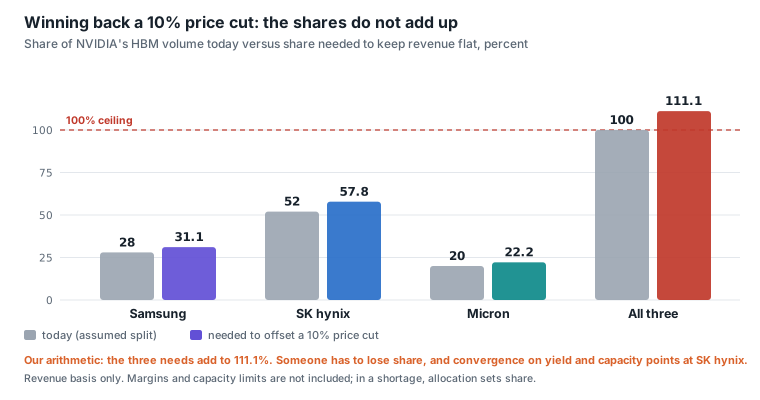
Under NVHBM the three makers build the same design, so share inside NVIDIA converges toward core 1c yield and capacity. A 10% price cut on NVIDIA volume costs Samsung $3.0 billion to $4.6 billion, SK hynix $5.5 billion to $8.5 billion and Micron $2.1 billion to $3.3 billion, across the 37% to 58% demand range. To make up the revenue with share alone, Samsung needs 3.1 more points, SK hynix 5.8 and Micron 2.2.
Those needs add to 111.1 points. That cannot happen, because shares add to 100. Someone gives up share, and convergence on yield and capacity points at SK hynix, which holds the largest share (52%) and so has the most to give back. In other words, SK hynix is likely to lose on price and on share, while Samsung and Micron can cover a price cut with small share gains. This is revenue only. It ignores margins and capacity limits, and in the 2027 to 2028 shortage allocation sets share.
What would change our reading
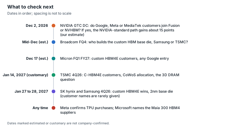
| Date | What to read | Default | What would move us |
|---|---|---|---|
| December 2, 2026 | NVIDIA GTC DC: NVHBM and Fusion partners, whether Google, Meta or MediaTek customers are in, and Feynman memory | No new large partner | Google or Meta named: the NVIDIA-standard path rises about 15 points (our estimate), and Broadcom and Samsung are marked down together |
| Mid-December (estimated) | Broadcom fiscal fourth quarter: AI revenue, custom chips by customer, HBM and packaging remarks | HBM structure not mentioned | A Samsung base die named supports the non-NVIDIA standard camp. A custom base die with TSMC reopens the design-partner path |
| December 17 (estimated) | Micron fiscal first quarter: custom HBM4E customers, ASIC share | ASIC customer growth | Google named: we revise the allocation assumptions |
| January 14, 2027 (customary) | TSMC fourth quarter: CoWoS allocation, C-HBM4E adoption, 3D DRAM question | Not mentioned | More custom base-die customers: the design-partner path rises about 5 points (our estimate) |
| January 27 to 28, 2027 | SK hynix and Samsung fourth quarter: custom HBM4E wins, 2nm base die | Customer names withheld | A Samsung win with Google or Broadcom supports the two-track path |
Data notes
- Supplier splits inside each buyer come from anonymous press reports, and Google’s 60% for Samsung dates from the HBM3E era. We do not know the HBM4 or 4E split. Read the results as order and range.
- NVIDIA’s 2027 demand share is estimated anywhere from 37% to 61%, because estimates mix bit demand, contracted volume and shipments. We computed with the 37% and 58% ends and did not pick a midpoint.
- Many items were confirmed through search summaries, not by opening the pages. The AMD and Samsung agreement is the only primary-source supply item. We did not open the original announcements for NVIDIA’s investments in Marvell and MediaTek, and the Marvell and Microsoft Maia 300 link is unconfirmed. Meta’s TPU purchase is at the negotiation stage in reports.
- Market size, base-die value share and demand shares are assumptions carried through the whole analysis. Paths, odds and the signs in the scorecard are our subjective judgment. The scorecard was made by one model family and was not cross-reviewed. We recomputed the 16 exposure cells and the price lines, and they match our research note.
- Counterpoint’s growth multiple for ASIC HBM demand comes from a headline we could not open (bot check), so we state it only as many times over.
- We found no Broadcom statement on base dies, no list of SPHBM4 supporters, and no confirmed HBM4 supplier for Meta or Microsoft Maia 300.
Sources:
- AMD: Samsung and AMD expand strategic collaboration
- NVIDIA blog: NVLink Fusion and NVHBM (2026-08-26)
- Tom’s Hardware: NVIDIA custom NVHBM, 30% more bandwidth, 15% less power
- StorageReview: NVHBM moves the memory controller into the HBM stack, Trainium4 first
- Counterpoint: The trillion-dollar bottleneck, NVIDIA’s NVHBM fight for the base die
- Counterpoint: HBM demand for AI server compute ASICs
- Blocks and Files: NVIDIA sidesteps the JEDEC HBM standard
- Tom’s Hardware: JEDEC SPHBM4 standard
- Tom’s Hardware: TSMC and GUC on HBM4, HBM4E and C-HBM4E base dies
- Tom’s Hardware: NVIDIA invests $2 billion in Marvell
- DCD: NVIDIA invests $2bn in Marvell
- Network World: NVIDIA invests $3.5B in MediaTek
- HotHardware: NVLink Fusion and the MediaTek deal
- ServeTheHome: NVLink Fusion tapped for AWS Trainium4
- TechRadar: NVIDIA pumps $2 billion into Marvell
- Tom’s Hardware: Marvell custom HBM solution
- Tom’s Hardware: Custom AI ASICs examined, from Broadcom to MTIA
- Tom’s Hardware: Meta’s four new MTIA chips
- TechRadar: Meta and Google could sign a mega AI chip deal
- TechEnclave: Microsoft announces Maia 300
- Korea Times: SK hynix becomes sole HBM supplier for Microsoft AI chips
- TrendForce: Samsung reportedly supplies 60% of Google TPU HBM3E
- TrendForce: Samsung HBM4 beats expectations in Broadcom test
- TrendForce: SK hynix leads custom HBM4E push
- TrendForce news (2026-09-18)
- Tom’s Hardware: Google reportedly books Intel for more than 3 million TPUs in 2028
- SamMobile: Samsung and OpenAI HBM supply
- NAND Research: Qualcomm AI200 and AI250
- Tom’s Hardware: Intel Crescent Island
- Profesional Review: NVIDIA to control 37% of HBM in 2027
Two questions for the comments.
1. Who will NVIDIA name as an NVHBM or Fusion partner at GTC DC on December 2? A. Neither Google nor Meta. B. Meta only. C. Google only. D. Both.
2. Which memory maker has the most to lose from standardized base dies? A. SK hynix. B. Samsung. C. Micron. D. None of them, because this is all price power at NVIDIA.
This is for research and information only, not investment advice. Probabilities, ranges and signs are analytical assumptions, not trading instructions or individual portfolio decisions. Figures are dated data. Anthropic, which makes the Claude model we used to collect sources and edit this post, is a large user of Google TPUs and AWS Trainium, both discussed here. We used public material only and do not judge the size of that effect.